


Mechatronics Fundamentals - Microcontrollers
Algae Update 10
There are 2 ways to communicate binary data.
Parallel = multiple bits at a time
Serial one bit sent at a time.
Parallel communication requires more transmission and receiving wires than serial (which can be implemented with just 3 wires). Parallel communication used to be popular because of the higher communication bandwidth and slower processing speeds of computers. Now that processors are orders of magnitude faster, the simplicity of serial has outweighed the bandwidth penalty. Now serial is used almost exclusively. Below is an example of parallel vs serial communication.

Inter-device communication can be synchronous or asynchronous. Synced has data in a continuous stream at a constant rate. This means that both the transmitter wire (TX) and the receiving wire (RX) devices must run at the same clock rate.
Asynchronous data is sent as needed, so no continuous stream. Clocks can be running at different rates, but devices need the same data (or baud) rate. The method of synchronization is through the start and stop bits.
Digital communication for MCUs is commonly done using async serial interfaces. Specifically, this is the universal asynchronous receives transmitters (UART) hardware device. Most modern microcontrollers have one or more onboard UARTs built in.
For 1-way communication, you need 2 wires: signal and ground
for 2-way communication you need 3 wires: signal out (Tx), signal in (Rx), and ground.
To send a byte (8 bits) of data, we must send 8 bits individually, plus a start and stop bit. The total would be 10 bits for each byte of data we send.
Baud Rate
The number of bits transmitted per second is represented by Time = 1/baud rate. For bytes per second = baud rate/10 (since you need 10 bits for 1 byte to transfer). Baud rate is set during serial communication configuration. Both devices must use the same baud rate. The tradeoff is higher baud rate —> higher communication speed and lower baud rate —> higher accuracy.
Typical baud rate (bits/sec): 9600, 57600, 115200
TTL Serial Communication
UART is a hardware device that implements transistor-transistor logic (TTL). TTL means communication means 3.3V or 5V is logic high, and 0V is logic low. 1 byte transmitted at a time is called a “frame”. Here you send the least significant bit (LSB) first and the most significant bit transmitted last). Below is an example with a byte of 01001011.
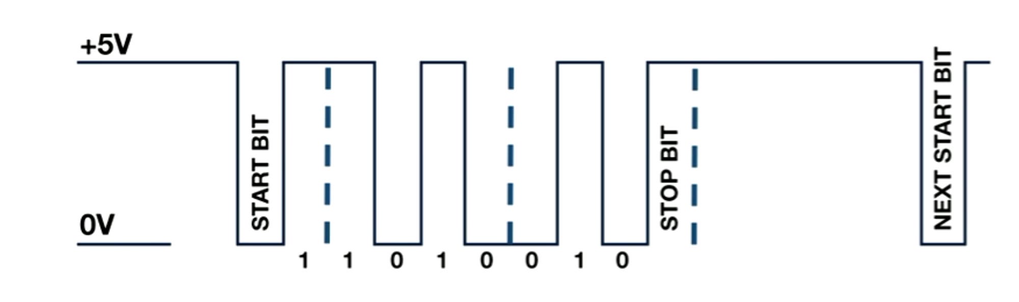
Because the signal is digital you can be at either 0 or 5V. Signal starts are 5V when there is no communication and when you have a start bit you go down to 0 volts. It then goes back to 5V after a bit of time. Then you go from LSB to MSB until you get to stop bit. You then stay at 5V until the next start bit. You can take as long to start the next frame because information does not need to be continuous.
Serial Interfaces and UART communication
Once the start bit is detected (logic high goes to logic low), the receiver waits for 1.5 * T (bit time) and samples line 9 times at T sec intervals to read data.

How Baud Rate Affects Accuracy
How long does it take to transmit each bit if the baud rate is 9600? How many bytes are transmitted each second?
Bit speed = 1/9600 = 104.2 microseconds Bytes per sec = 9600/10 = 960 bytes per sec
If the clock speed on a receiving device was off 4 microseconds from the transmitting device, how would that affect your data reading?
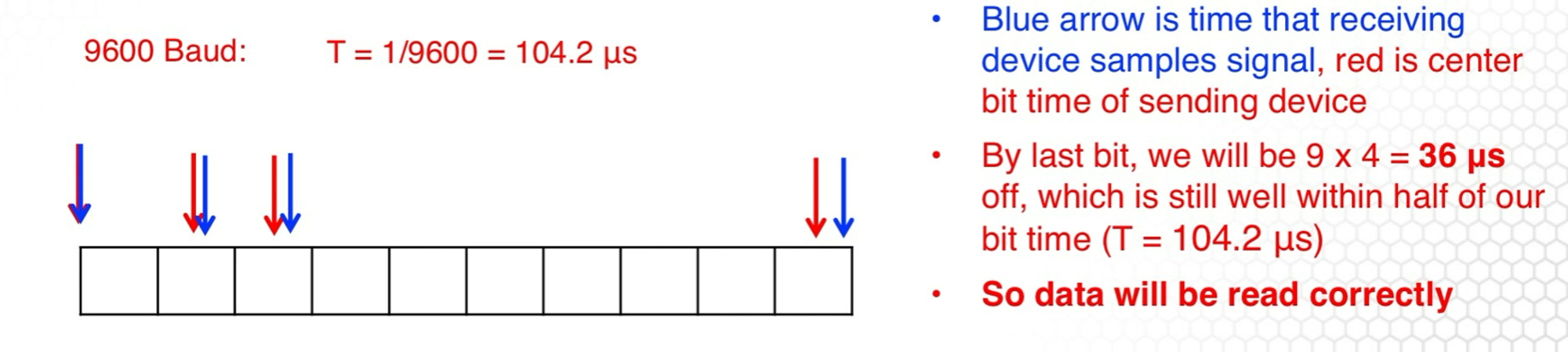
As long as your data is in the same box (delay is lower than the value of T) then you are good because it reads the same data. If you were reading data with a 38,400 baud with a 4-microsecond delay for the receiver, what would happen?
Baud rate = 1/38600 = 26.0 microseconds/bit.
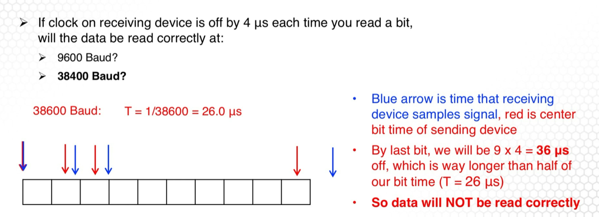
The delay of receiving the device is larger than T. Your data will not be read correctly. Clock rate mismatches between sending and receiving devices are the main factor that limits the Baud rate. Current microcontroller use clocks (digitally-controlled oscillators) that limit Baud rates to around 100,000 bit/sec.
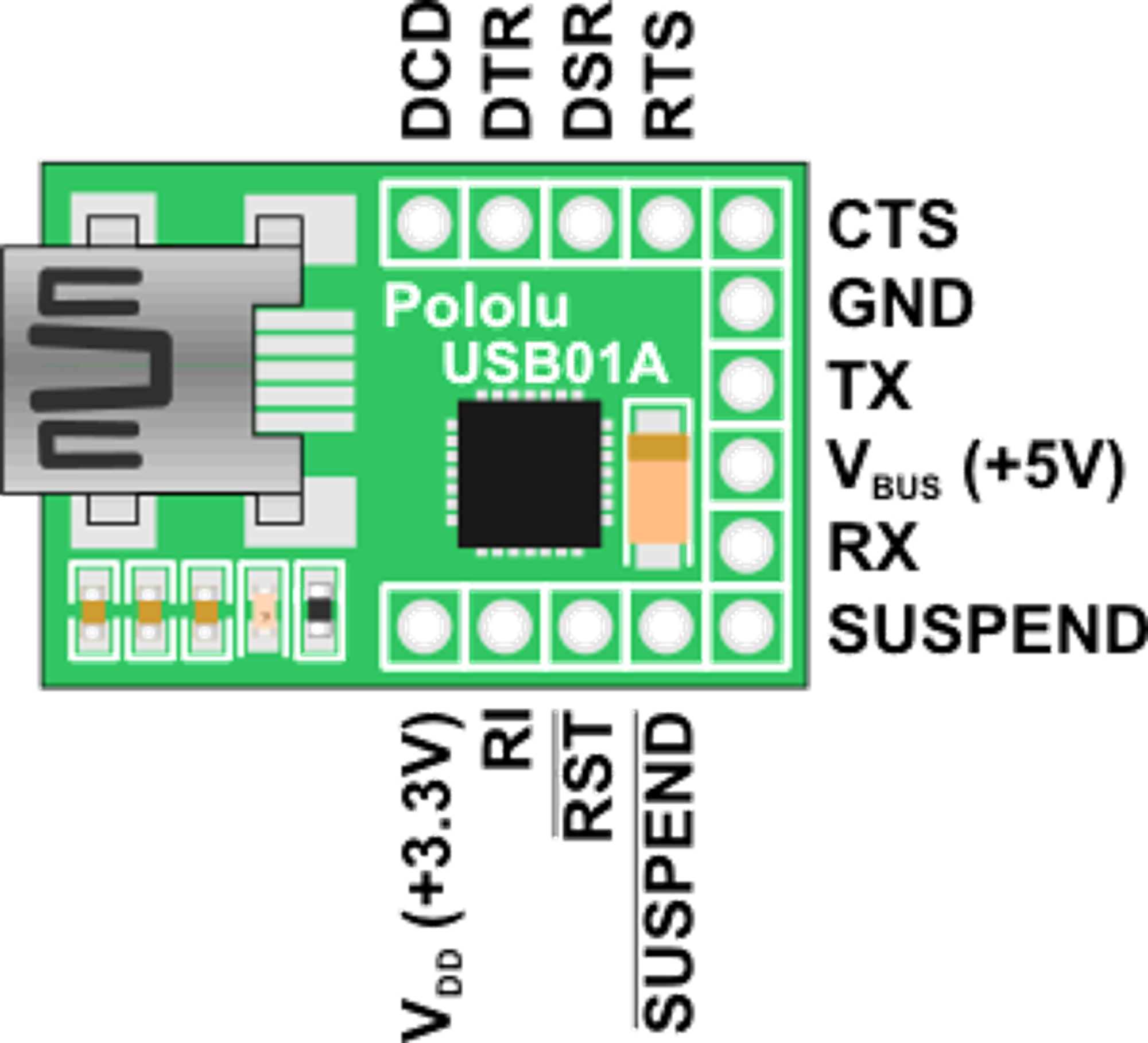
When sending data from MCU (UART) to the computer via USB. We need to convert a TTL serial signal to a USB with adapter boards. The adapter boards have pins for TTL serial Transmission and receiving wires (TX and RX). There is a mini-USB connected on the other side. Example below.
UART Sending Operation
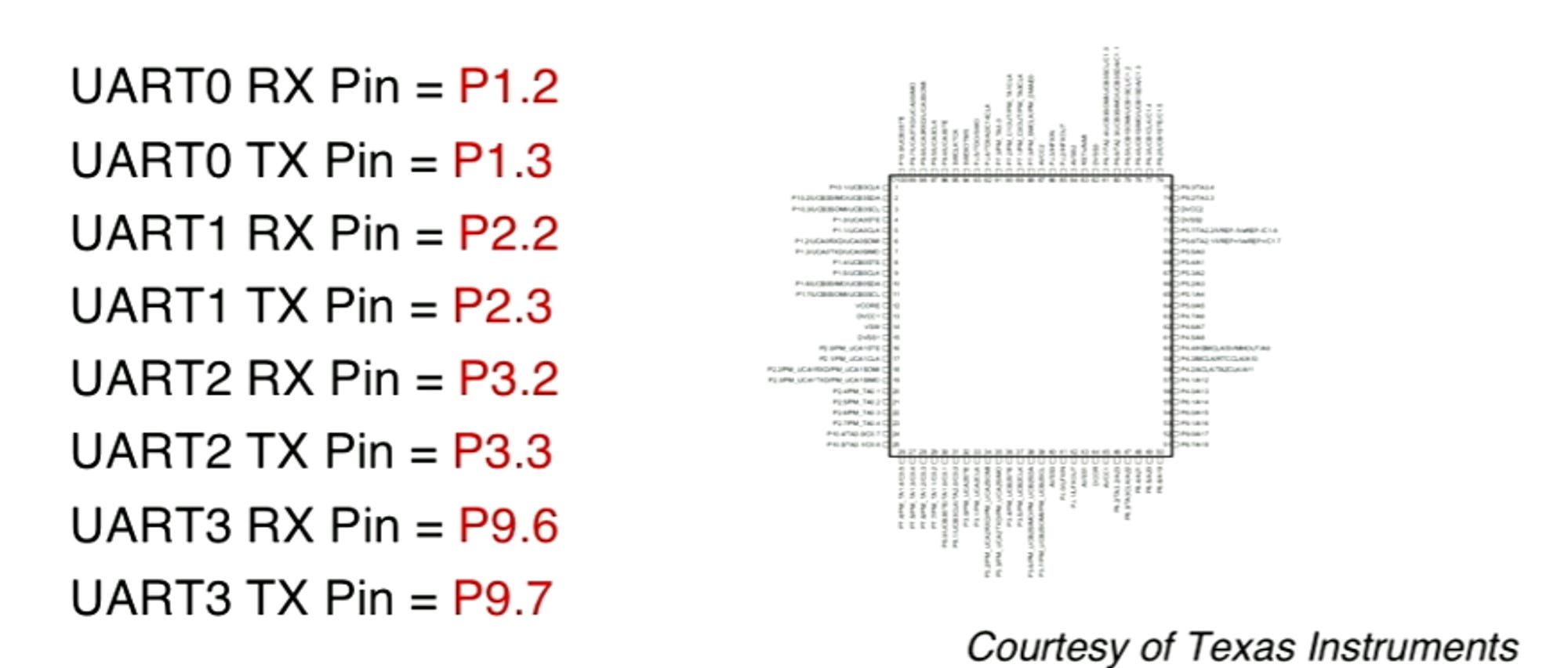
UART is a hardware device that implements TTL serial protocol. The explanation below is based on the MSP432 microcontroller that has 4 UARTs. From the datasheet, we find the transmission and receiving pins. The image on the right shows the 100 different pins available. All of their functionalities can be found in the datasheet of the microcontroller.
UART data is transmitted one byte at a time. The example below is specific to MSP432, but another microcontroller will have similar registers in the datasheet.
Step 1: Byte is written to Transmit buffer (TXBUF) registers.
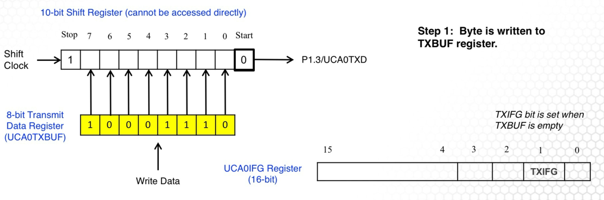
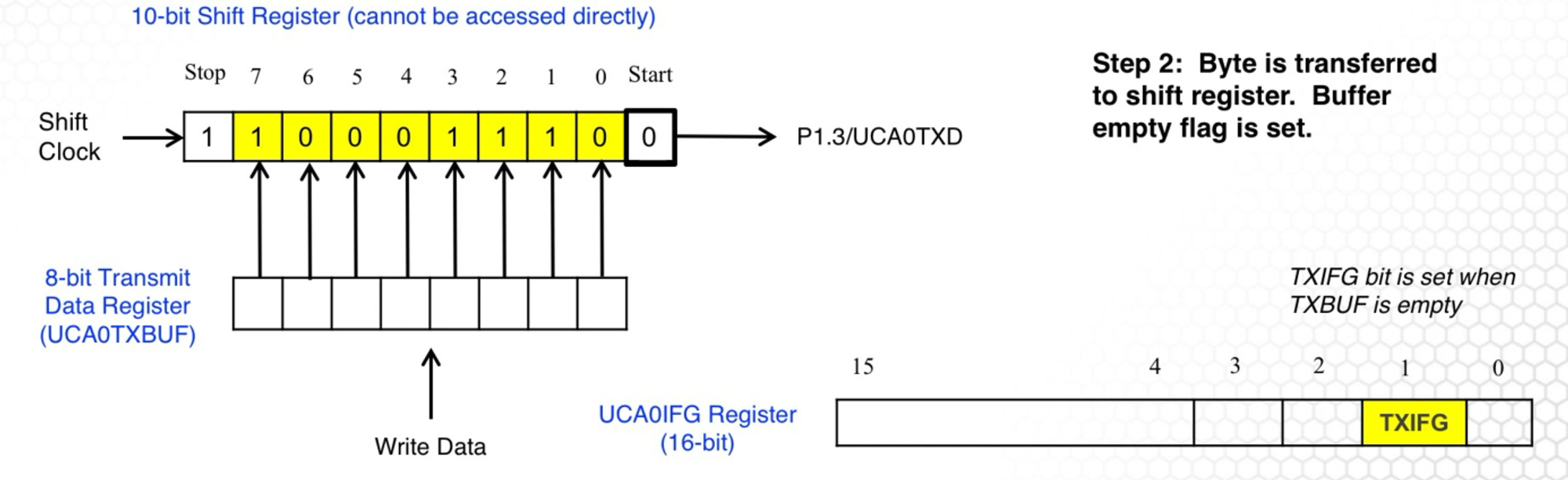
Step 2: Byte is transferred to shift register. Shift holds the byte that is actively being sent. The transmit interrupt flag (TXIFG) bit is set high. That bit is set high indicates that the transmit data register is empty and you can write another byte to the TXBUF data register without overwriting something that is already there. To prevent this problem we can use a transmit interrupt.
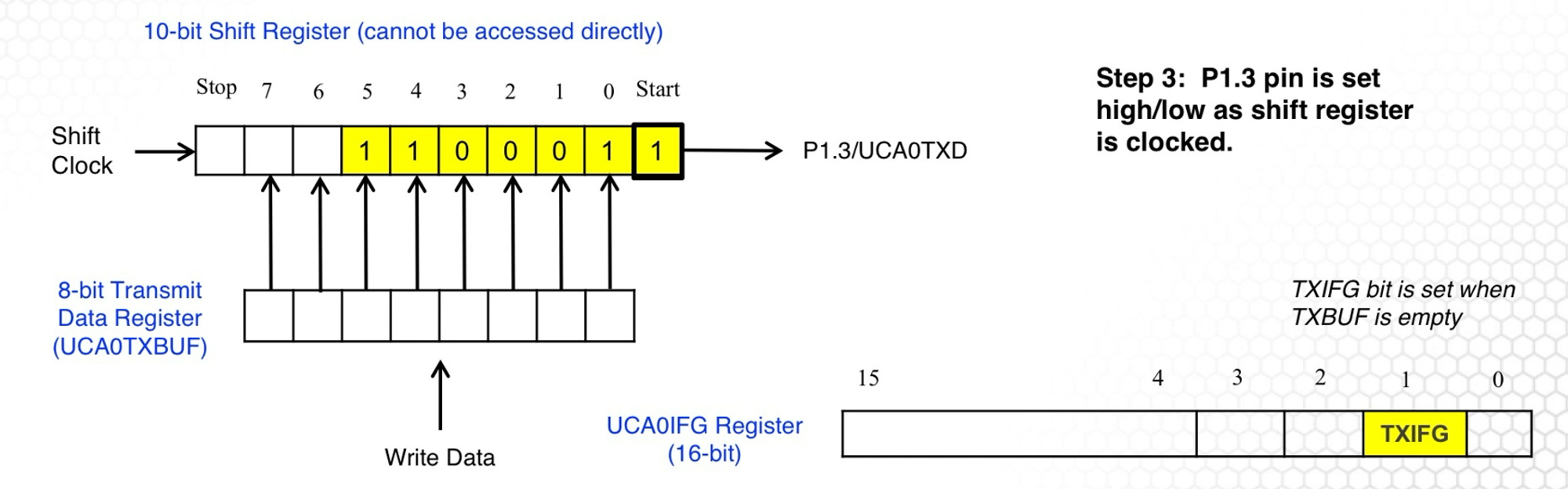
Step 3: The data is shifted over by the shift clock. Every time the shift clock provides a pulse that registers the data is moved over 1 bit. The associated transmit line pin 1.3 for UART module 0 is set to the bit value shown in the highlighted square.
The data is shifted out and the pin is set high or low (1 or 0) depending on the bit value. The data gets shifted at the baud rate.
Step 4: Once the data is fully shifted then the line is set to its normal high position (because of the next start bit) and our transmit data register can be filled again with new data, and we can keep sending data this way.

Note: To send more than 1 byte of data you need to break down large amounts of data into 1-byte chunks.
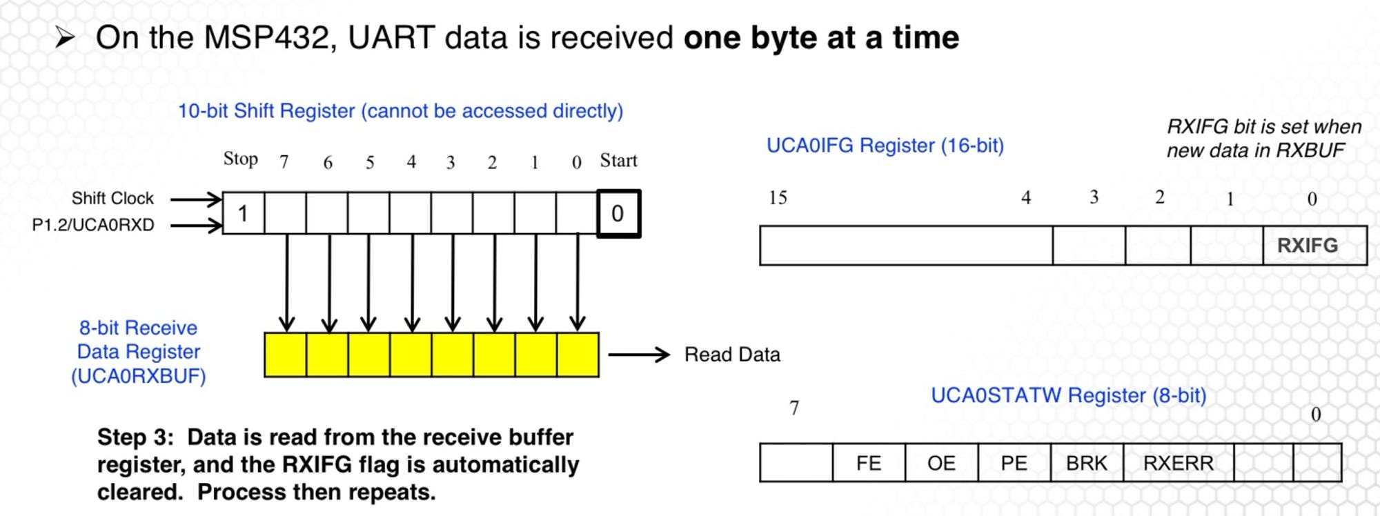
UART Receiving Operation
Similar to transmission we can only receive 1 byte of data at a time. The UART senses that the start bit was set so it will start to shift the UART received shift registers. The clock pulse starts shifting data into the data shift register. The received data register now holds the byte that was sent.

At the same time, the receive interrupt flag gets set. It is bit 0 in the IFG register. That bit tells that there is data available in the receive data register or receives buffer that we can go get.
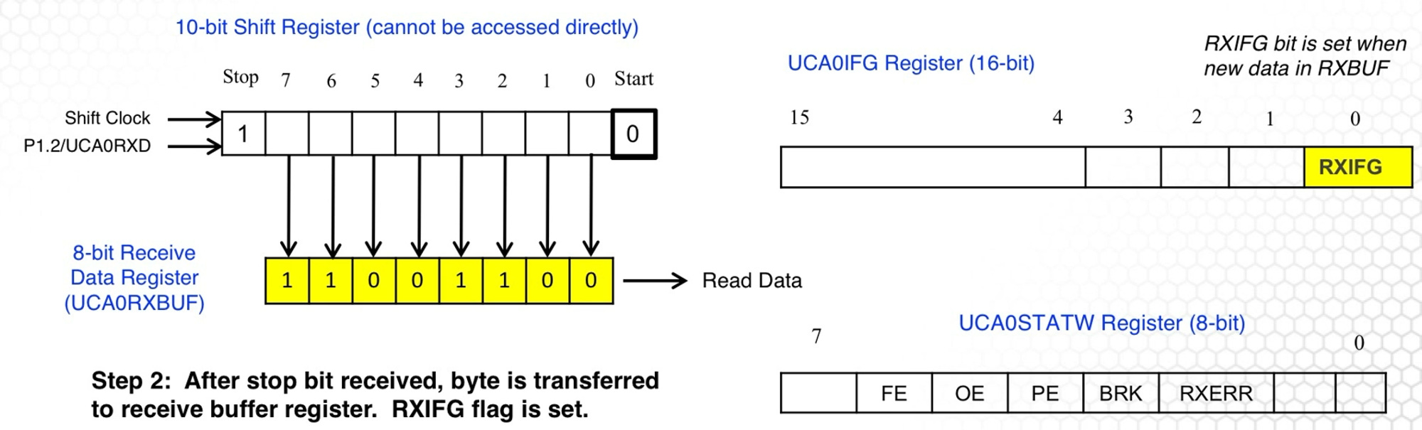
Our program will read that data into a variable. Once we read that data the receive interrupt flag automatically goes to 0 so it is automatically cleared, and then we are ready to receive another byte.
There are some ways it can go wrong. The most common is overflow error - suppose both receive buffer and shift register are full when another byte comes in. To keep the shift register clear, the UART device is going to take that byte of data and overwrite what’s in the receive buffer.
It means you didn’t keep up with reading the data fast enough. You need to make sure that as soon as that receive interrupt flag goes high you read the data. The best practice is to use a UART receive interrupt to make sure data is read on time.
I^2C (or I2C) protocol
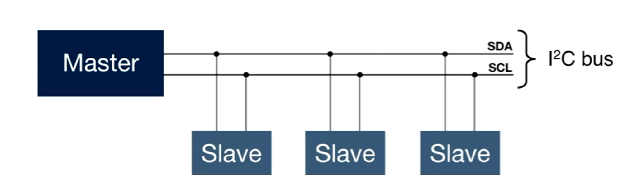
Sensors communicate with microcontrollers commonly with the I^2 C protocol. It stands for the inter-integrated circuit. Used to communicate between microcontrollers, sensors, and actuators.
Key terms for protocol
SDA: Data wire. Data bits flow along this line
SCL: Clock wire. Transmits clock signal which is used to synchronize data transfer.
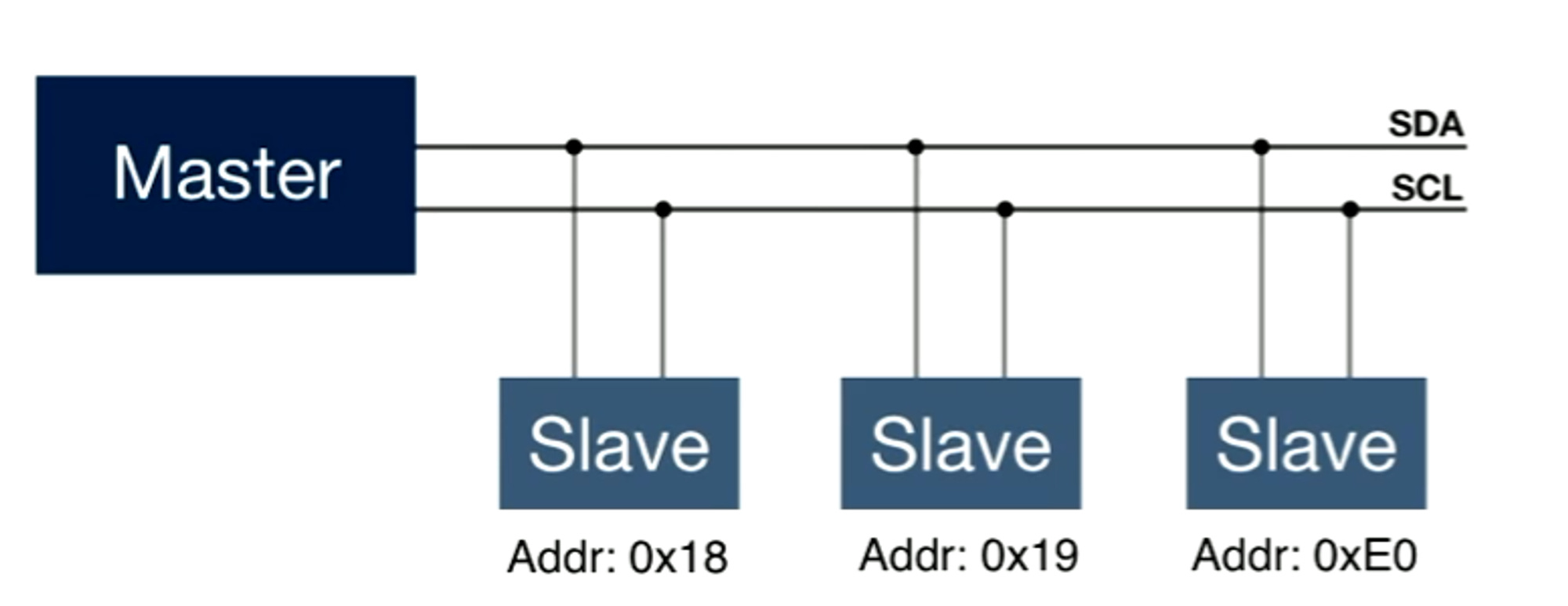
Master: Device (usually MCU) which controls clock (SCL) line. Usually only 1 per bus (collection of SDA and SCL wires).
Slaves: Devices (MCUs, sensors, actuators) that monitor SCL and communicate on SDA.
When implementing a I^2C bus, pull-resistors (which are part of an open collector circuit) which are needed on each line to set the logic level being used (either 3.3V or 5V) across all of the different circuit lines (SDA and SCL).
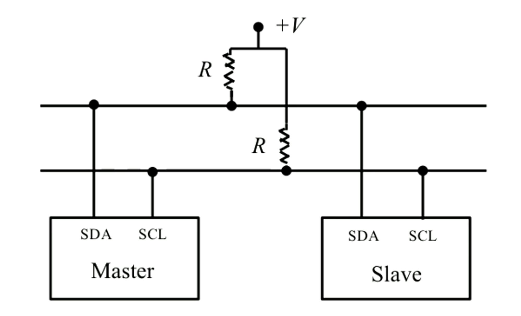
Some microcontrollers have SCL and SDA lines already tied with 3.3V or 5V via an internal resistor, so no need to use an external one.
Initiating Data Transfer with I2C
To initiate data transfer only the Master can do it, slaves respond to the master's request. Data can be sent in either direction. Each slave has a unique address assigned to it. Usually 7 bits, but sometimes 10 bits binary number (this you can set address values of each slave device).
The address that you see for each slave is a hex number, which is a different method of representing numbers called the hexadecimal system, which is a way to represent binary in short form.
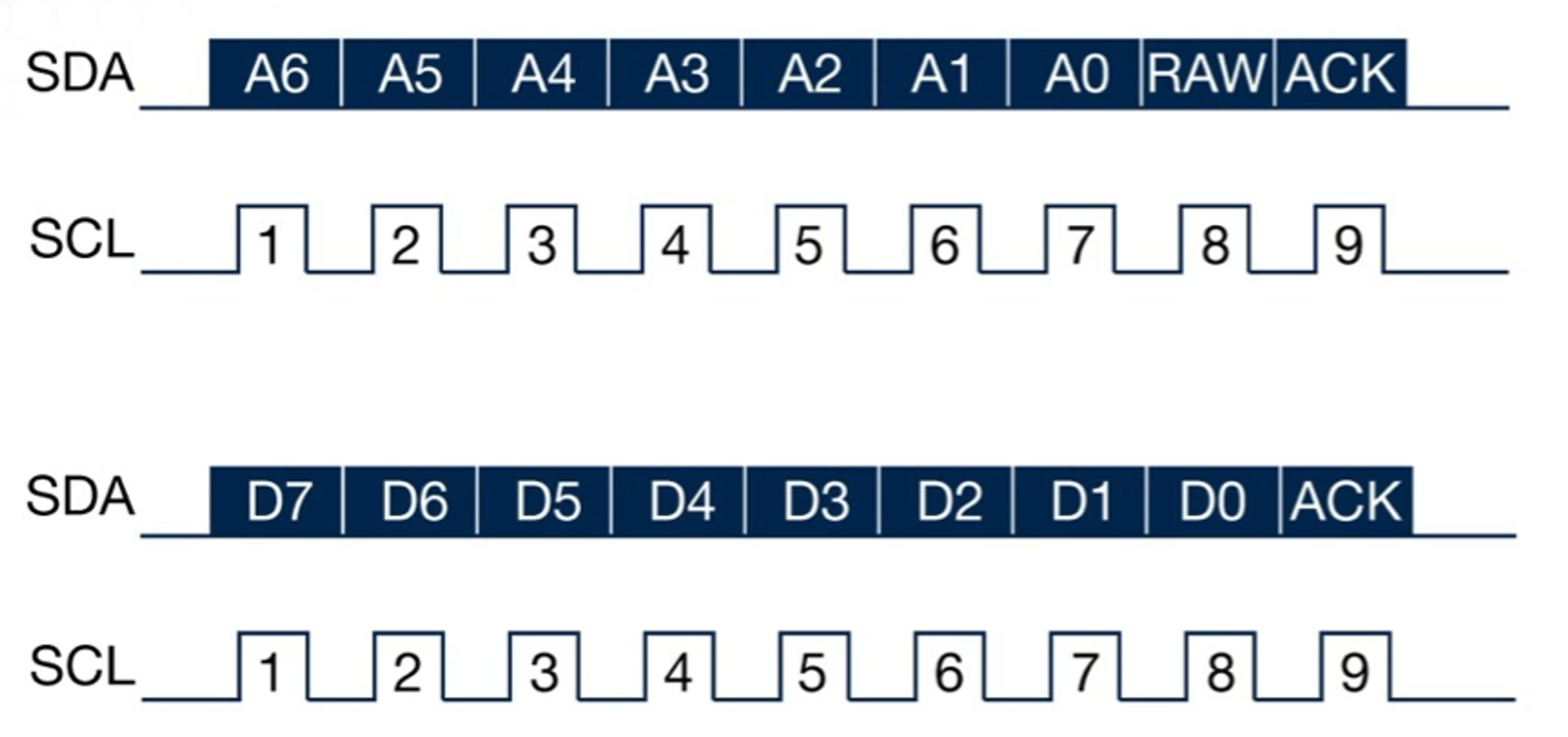
Data for I2C communication is sent in messages. Each message is broken up into frames. The address frame specifies which slave should be communicating. Data frames hold binary data that is transmitted with 1 byte of data.
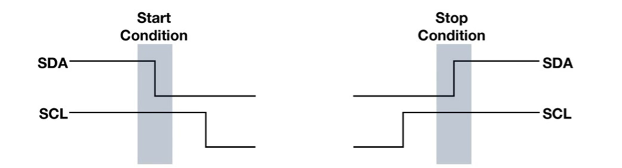
Each message starts with Start Condition and ends with End Condition.
Start: SDA line changes from high to low while SCL (clock line) is held high.
End: SDA line changes from low to high while SCL (clock line) held high).
The only time SDA is allowed to change is when SCL remains constant. Below is a visual example.
Every frame (address and data) ends with ACK or NACK bit. If the frame was successfully received by receiving device, the ACK bit was sent (0). If the frame was not successfully received or understood, receiving device sends NACK bit (1). ACK stands for acknowledged and NACK is not acknowledged.
There is also a read/write bit: A single bit specifying whether Master is sending data to Slave (bit value would be 0), or Master is receiving data from Slave (bit value would be 1). A visual example of different components in a message is below.

Each bit in the frame is transmitted when a clock pulse occurs. Master device sends clock pulses on SCL line, then either Master or slave sets SDA line high or low to send data (either 0 or 1).
Many I2C communication devices have internal registers, meaning a slave has its own microprocessor or microcontroller that has its own registers that the master can either read from or write to. When we send data out we don’t just send it to the slave address, but we’ll need to send a slave register address. This can increase the complexity of the programming. Example below.
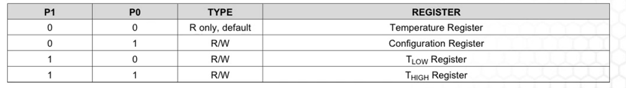
These are images from the datasheet of a temperature sensor that communicates with I^2C. The sensor has a few registers. The temperature register holds the temperature value and the configuration register which holds some configuration bits for how we want the sensor to operate. The data sheet shows the I^2C protocol to an internal register. You send the address and then in the first data frame, it is shown that you are sending to the registered address you want to send to.

Once the slave or temperature sensor in this case knows where you are trying to send data to then you can go ahead and send that. Depending on the type of sensor you have, the protocol might be a bit more complicated than what is mentioned for UART above. Not only do we need to send data to a slave, but we also need to send it to a particular register on the slave.
SPI Communication Protocol
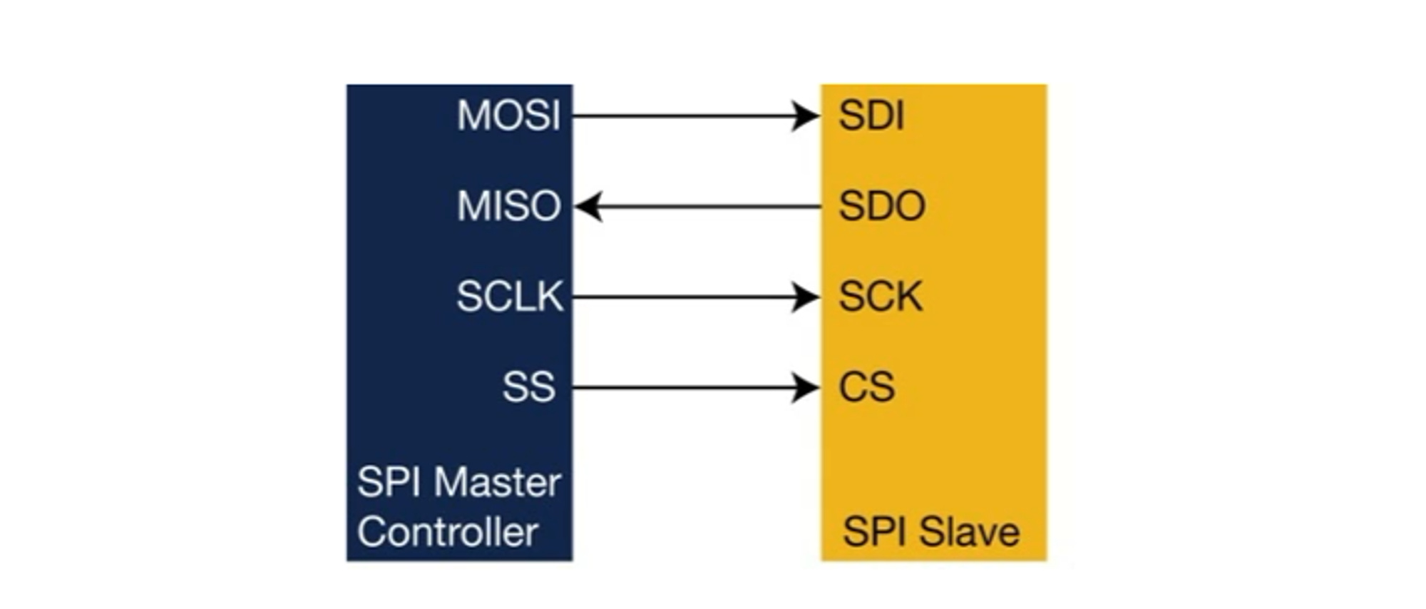
SPI common protocol used for embedded devices. SPI uses the same idea as I^2C of master and slave devices. There are 4 wires to connect 2 SPI devices.
SCLK: Clock wire. This transmits a clock signal which is used to synchronize data transfer.
MOSI: Master out slave in the wire. Transfers data from the Master to the slave device.
MISO: Master in slave out the wire. Transfer data from slave to master
SS: Slave select wire. Activates slaves for communication.
Regardless of how many slaves are there. The same SCLK, MOSI, and MISO are used, but each slave they have theirs on SS wire.
How to add slaves for SPI
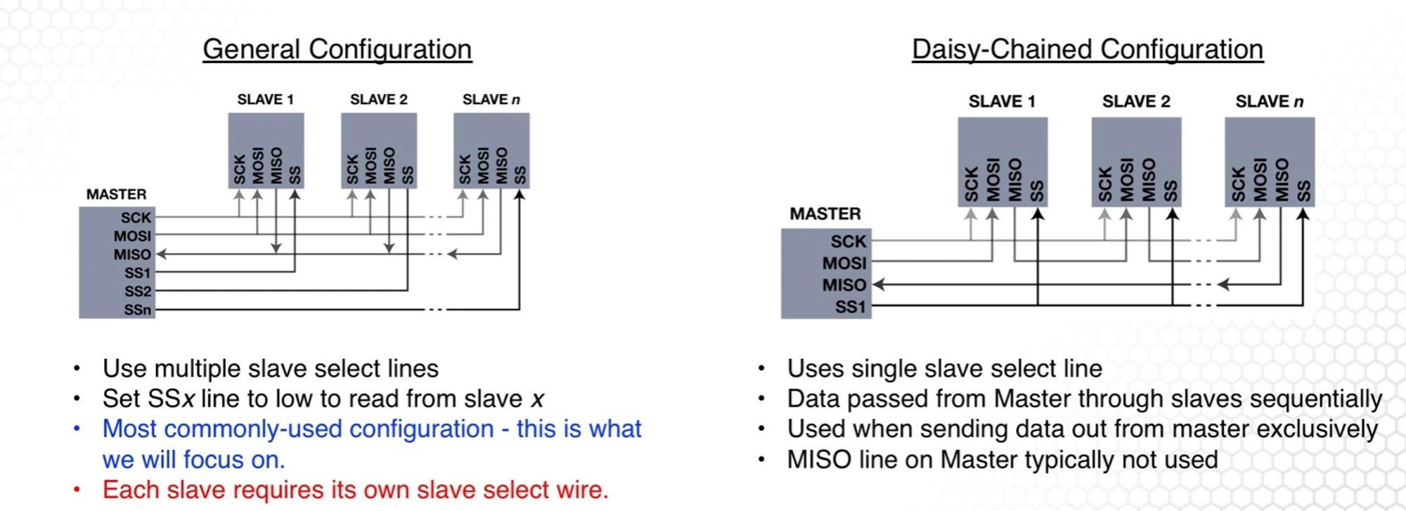
Daisy has less wires, but requires much more data transmission which is not useful the applications we need so just focusing on master-slave configuration. Like other protocols it works 1 byte at a time.
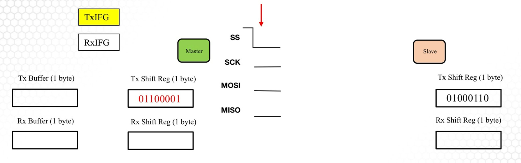
Example of SPI with general configuration.
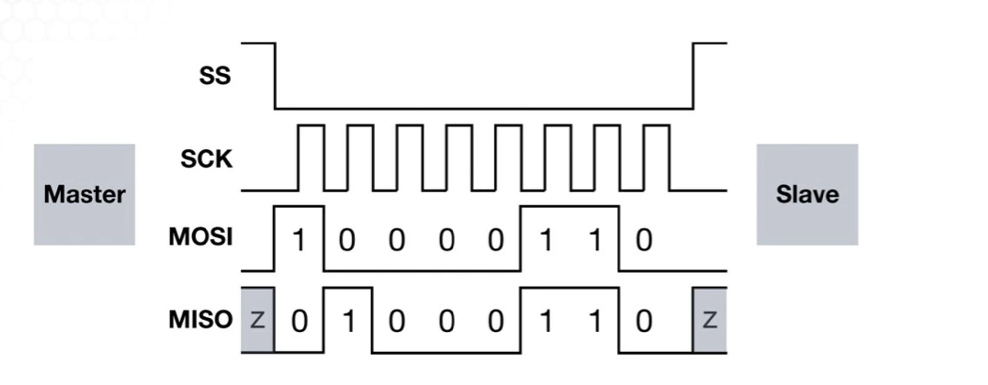
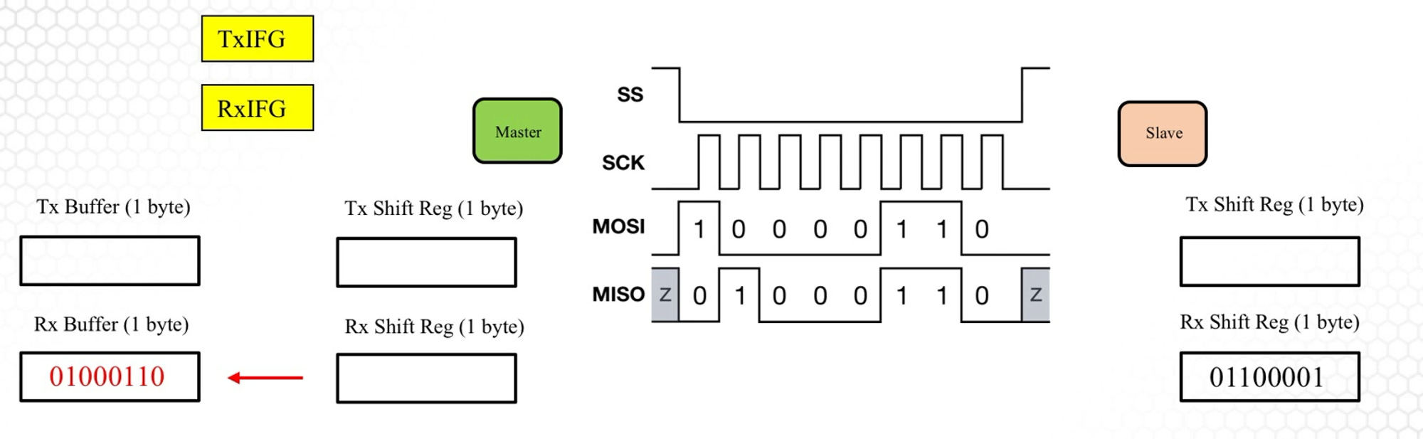
Slave select line is held high when no communication is occurring. Master then holds the slave select line low to say I’m ready to communicate with you. Master sends 8 clock pulses to transmit 1 bit of data, but it is always transmitted in both directions through the Master out slave in, and master in slave out.
This means that both the master and slave need to receive and transmit regardless of operation. There is no read-only or write-only operation. the bit has to go in both directions.
Process of Sending and Receiving data with SPI
Step 1: Master puts data into transmit buffer register. If you want a master to receive from a slave you will need to send out data. You can send a byte full of 0’s which the slave can ignore.
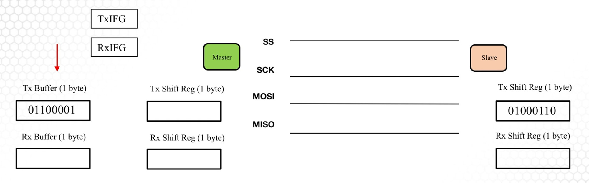
Step 2: Data from the transmit buffer to places in the transmit shift register. The transmit interrupt flag goes high, telling us that the transmit buffer is free if we want to write more data.

Step 3: The master holds the slave's select line low to tell the slave that communication is about to start.
Step 4: The master then gives eight clock pulses and the data gets shifted from along the MISO line and moves right into the receive shift register on the master. The MOSI line takes the data from the master to the slave, and the result is placed in the receive shift register on the slave. Note: SPI usually sends the most significant byte first.

Step 5: The data in the receive shift register is moved to the receive buffer, setting the receive interrupt flag high, letting us know that we can go get our data. Step 6: Finally, the master also raises the slave select line high, indicating the end of the transmission.
Comparison between UART, I^2C, and SPI
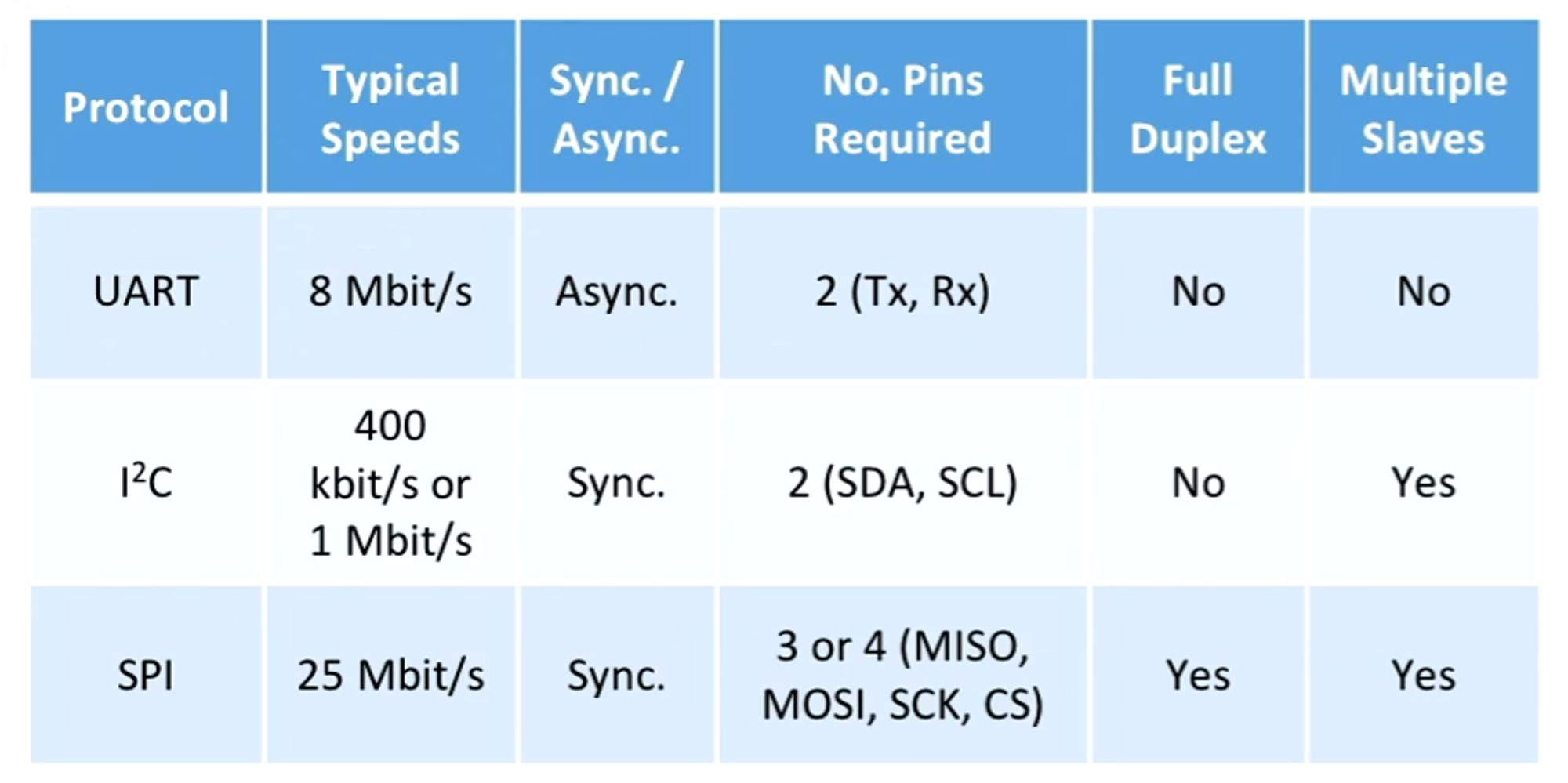
SPI and I2C are used for communication with MCUs, sensors, and actuators. UART is used for communication between MCUs and computers. SPI is the fastest, but you need more wires to connect the devices. This is needed for applications that require high speeds. The increased speed complex from the full duplex model, allows you to receive and transmit data at the same time. For my purposes, I^2C should be sufficiently fast, and it includes a less complex design because you only need 2 wires.